

Engineered Plastic for Semiconductor and Electronics Market to Reach USD 2.78 Billion by 2032 at 7.5% CAGR
Global Engineered Plastic for Semiconductor and Electronics market size was valued at USD 1.42 billion in 2024. The market is projected to grow from USD 1.56 billion in 2025 to USD 2.78 billion by 2032, exhibiting a CAGR of 7.5% during the forecast period.
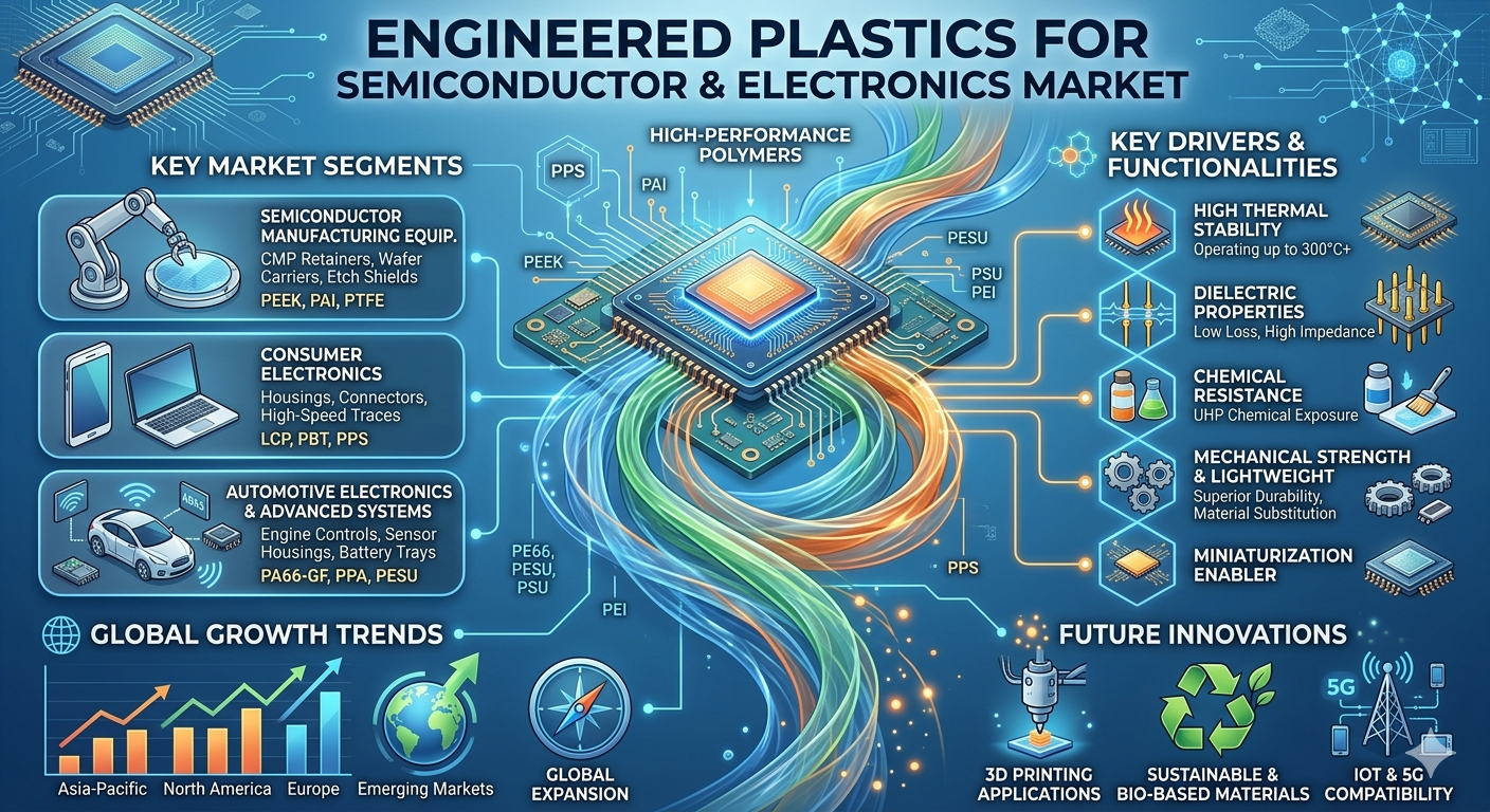
Engineered plastics, high-performance polymers engineered for exceptional thermal stability, chemical resistance, and superior mechanical properties, have become indispensable in the semiconductor and electronics industries. These materials—including stalwarts like PEEK, PTFE, and PVDF—are the unsung heroes behind the relentless march of technological advancement. Their ability to withstand extreme processing temperatures, harsh chemical environments, and provide precise electrical insulation makes them critical for manufacturing, testing, and protecting sensitive electronic components. As the demand for smaller, faster, and more powerful devices intensifies, the role of these advanced materials becomes increasingly paramount, moving from a supporting act to a core enabler of innovation.
Get Full Report Here: https://www.24chemicalresearch.com/reports/266384/global-engineered-plastic-for-semiconductor-electronics-market-2024-2030-287
Market Dynamics:
The market is navigating a landscape defined by powerful, sustained growth drivers, alongside specific challenges that the industry is actively working to overcome, all while eyeing substantial future opportunities.
Powerful Market Drivers Propelling Expansion
-
The Unrelenting Demand for Miniaturization and Advanced Packaging: The semiconductor industry's pursuit of Moore's Law, though evolving, continues to drive the need for materials that can perform in increasingly demanding fabrication processes. Engineered plastics are crucial in advanced packaging technologies like Fan-Out Wafer-Level Packaging (FOWLP) and 3D IC stacking, where their low coefficient of thermal expansion (CTE) and high thermal stability prevent warping and delamination. For instance, certain high-performance polymers maintain dimensional stability at temperatures exceeding 260°C, which is critical for lead-free soldering processes. The global semiconductor fabrication materials market, a key driver for engineered plastics, is itself projected to surpass $70 billion by 2025, creating a massive pull for high-purity, reliable materials.
-
Proliferation of Electric Vehicles and 5G Infrastructure: The explosive growth in electric vehicle production and the global rollout of 5G networks represent two of the most significant growth vectors. In EVs, engineered plastics are used in battery modules, power electronics, and sensors, where they provide flame retardancy (achieving UL94 V-0 ratings) and resistance to coolants and battery acids. The 5G era demands materials with low dielectric constants and dissipation factors for high-frequency circuit boards and antenna systems. Materials like PTFE and certain liquid crystal polymers (LCPs) are essential for minimizing signal loss at frequencies above 28 GHz, enabling the high-speed, low-latency communication that defines 5G technology.
-
Heightened Focus on Reliability and Yield in Semiconductor Manufacturing: In the ultra-precise world of semiconductor manufacturing, contamination is the enemy. Engineered plastics used in wafer carriers (FOUPs), chemical handling systems, and wet benches must exhibit ultra-low levels of extractables and leachables to prevent yield-killing defects. Manufacturers are increasingly adopting high-purity grades of PFA and PVDF, which can reduce metallic contamination to parts-per-billion levels. This focus on yield enhancement is critical, as a single failed wafer in an advanced node fab can represent a loss of tens of thousands of dollars, making the investment in premium materials a strategic necessity.
Download FREE Sample Report: https://www.24chemicalresearch.com/download-sample/266384/global-engineered-plastic-for-semiconductor-electronics-market-2024-2030-287
Significant Market Restraints Challenging Adoption
Despite their critical role, the adoption of engineered plastics faces economic and technical hurdles that require careful management.
-
High Material Costs and Supply Chain Vulnerabilities: The advanced synthesis and purification processes for polymers like PEEK and PEI result in costs that are 5 to 20 times higher than standard engineering plastics. This premium pricing can be a barrier for cost-sensitive applications. Furthermore, the supply chain for high-performance polymer precursors can be concentrated and susceptible to disruptions, as seen during recent global events. Price volatility for key raw materials like fluoropolymers can lead to cost increases of 10-15% annually, creating budgeting challenges for OEMs and fabricators who require price stability for long-term production planning.
-
Technical Challenges in Processing and Fabrication: The very properties that make these plastics desirable—high melting points and chemical resistance—also make them difficult to process. Machining PEEK or PTFE requires specialized tooling and expertise to avoid stress cracking and achieve the micron-level tolerances demanded by the semiconductor industry. Injection molding these materials often necessitates heated molds (often above 180°C) and sophisticated screw designs, increasing both capital equipment costs and the complexity of the manufacturing process. This high barrier to entry limits the number of qualified fabricators, potentially leading to longer lead times.
Critical Market Challenges Requiring Innovation
The path from material specification to finished component is fraught with challenges that demand continuous innovation.
One of the most persistent challenges is achieving and maintaining the extreme levels of purity required, particularly in wafer processing equipment. Even minute levels of ionic contamination can migrate and destroy semiconductor devices. Ensuring lot-to-lust consistency in virgin polymer is difficult, and the subsequent fabrication processes—machining, cleaning, and assembly—must be performed in controlled environments to prevent introducing contaminants. A single mishap in handling can render a batch of costly components unusable.
Additionally, the industry faces a growing need for material solutions that address emerging technological requirements, such as heat dissipation in high-power electronics. While engineered plastics are excellent insulators, there is increasing demand for grades with enhanced thermal conductivity to manage heat in compact devices. Developing such materials without compromising electrical insulation properties or processability is a significant R&D challenge that consumes substantial resources for material suppliers.
Vast Market Opportunities on the Horizon
-
The Next Frontier: Heterogeneous Integration and Chiplets: The industry's shift from monolithic chips to heterogeneous integration, where multiple smaller chiplets are combined in a single package, opens a new frontier for engineered plastics. These advanced packages require new types of substrates, interposers, and encapsulation materials that offer ultra-low moisture absorption and minimal stress. Materials with tailored dielectric constants and thermal properties are needed to enable the high-density interconnects between chiplets. This paradigm shift is creating a potential multi-billion dollar opportunity for material innovators who can meet these stringent new requirements.
-
Sustainability and Circular Economy Initiatives: As environmental regulations tighten and corporate sustainability goals become more ambitious, there is a growing opportunity for bio-based, recyclable, or lower-carbon-footprint engineered plastics. While performance cannot be compromised, developments in high-performance biopolymers and advanced recycling technologies for fluoropolymers are gaining traction. Companies that can successfully commercialize sustainable alternatives without sacrificing the critical performance characteristics stand to gain a significant competitive advantage, especially with environmentally conscious OEMs in Europe and North America.
-
Expansion into Emerging Applications: AR/VR and Advanced Medical Electronics: Beyond traditional computing and communications, new frontiers like Augmented and Virtual Reality (AR/VR) and implantable medical electronics demand lightweight, durable, and biocompatible materials. For AR/VR headsets, polymers like PEI are used for their high strength-to-weight ratio and ability to be molded into complex optical housing shapes. In medical electronics, materials must withstand repeated sterilization cycles and bodily fluids, creating a specialized niche for grades of PEEK and PVDF that are certified for biocompatibility (ISO 10993). These high-value segments offer margins that are often 20-30% higher than standard industrial applications.
In-Depth Segment Analysis: Where is the Growth Concentrated?
By Type:
The market is segmented into FEP, PEEK, PTFE, HDPE, PVDF, PEI, and others. Polyetheretherketone (PEEK) and Polytetrafluoroethylene (PTFE) currently dominate the high-value segment of the market. PEEK is favored for its exceptional combination of high temperature resistance, mechanical strength, and purity, making it ideal for wafer carriers and critical components inside fabrication tools. PTFE remains the gold standard for applications requiring the ultimate in chemical resistance and low dielectric loss, such as in high-frequency circuit boards and chemical-wet processing equipment.
By Application:
Application segments include Circuit Boards, Connectors, Insulators, & Nests, Fixtures, Hard Disk Drives, Integrated Circuits, Probe Cards, Test Sockets, and others. The Circuit Boards and Connectors, Insulators, & Nests segments collectively account for the largest market share. This is driven by the sheer volume of PCBs produced globally and the critical need for reliable, durable insulation and structural components in semiconductor testing and handling equipment. However, the Integrated Circuits application segment, which includes wafer fabrication components, is expected to see the highest growth rate, fueled by massive investments in new semiconductor fabs worldwide.
By End-User Industry:
While the primary end-user is the integrated Semiconductor and Electronics industry, it can be further broken down by application focus. The segment focused on semiconductor capital equipment—manufacturers of tools for chip fabrication—represents the most demanding and high-value segment. The consumer electronics segment is the largest by volume, driven by the production of smartphones, laptops, and other devices. The automotive electronics sector is the fastest-growing end-user, propelled by the electrification of vehicles and the increasing electronic content per car.
Download FREE Sample Report: https://www.24chemicalresearch.com/download-sample/266384/global-engineered-plastic-for-semiconductor-electronics-market-2024-2030-287
Competitive Landscape:
The global Engineered Plastic for Semiconductor and Electronics market is fragmented yet features several dominant players with strong technological expertise. The market is characterized by high barriers to entry due to the significant R&D investment and stringent quality certifications required. The top players—Victrex (UK), Solvay (Belgium), and Ensinger (Germany)—collectively hold a significant portion of the high-performance polymer segment, leveraging their extensive product portfolios and deep relationships with major semiconductor equipment manufacturers.
List of Key Engineered Plastic for Semiconductor and Electronics Companies Profiled:
-
Ensinger (Germany)
-
Boedeker Plastics (U.S.)
-
Victrex (UK)
-
Solvay (Belgium)
-
Evonik (Germany)
-
ZYPEEK (China)
-
Kingfa (China)
-
Craftech Industries (U.S.)
-
EPTAM (U.S.)
-
Mitsubishi Chemical (Japan)
-
Saint-Gobain (France)
-
Vanderveer Industrial Plastics (U.S.)
-
ERIKS Seals and Plastics (Netherlands)
-
TOHO KASEI (Japan)
-
E. Jordan Brookes (UK)
-
Vycom Plastics (U.S.)
-
Thyssenkrupp Materials (Germany)
-
BKB Precision (U.S.)
-
TOWA (Japan)
-
Plastic Distributors and Fabricators (U.S.)
-
Wah Lee Industrial Corp (Taiwan)
The predominant competitive strategy revolves around developing application-specific polymer formulations, achieving critical industry certifications (like SEMI Standard grades), and providing extensive technical support to customers. Vertical integration, from polymer production to precision machining, is also a key differentiator for leading companies aiming to control quality and supply chain reliability.
Regional Analysis: A Global Footprint with Distinct Leaders
-
Asia-Pacific: Is the dominant force in the market, accounting for over 60% of global consumption. This leadership is driven by the concentration of semiconductor fabrication, assembly, and testing facilities in countries like Taiwan, South Korea, China, and Japan. The region is both the largest producer and consumer of electronic goods, creating immense demand for engineered plastics throughout the supply chain. Massive government-led investments in domestic semiconductor production, particularly in China, are further accelerating regional growth.
-
North America and Europe: Together, these mature markets represent a significant share, characterized by high-value, innovation-driven demand. North America, home to leading semiconductor equipment companies and fabless chip designers, demands the highest-performance materials for R&D and leading-edge manufacturing. Europe maintains a strong position, supported by major chemical companies like Solvay and BASF, and a robust automotive electronics sector demanding high-reliability components.
-
Rest of the World: Regions like South America and the Middle East & Africa currently represent smaller markets but are poised for growth as electronics manufacturing continues to diversify geographically. Investments in infrastructure and a growing consumer base for electronics present long-term opportunities for market expansion.
Get Full Report Here: https://www.24chemicalresearch.com/reports/266384/global-engineered-plastic-for-semiconductor-electronics-market-2024-2030-287
Download FREE Sample Report: https://www.24chemicalresearch.com/download-sample/266384/global-engineered-plastic-for-semiconductor-electronics-market-2024-2030-287
About 24chemicalresearch
Founded in 2015, 24chemicalresearch has rapidly established itself as a leader in chemical market intelligence, serving clients including over 30 Fortune 500 companies. We provide data-driven insights through rigorous research methodologies, addressing key industry factors such as government policy, emerging technologies, and competitive landscapes.
-
Plant-level capacity tracking
-
Real-time price monitoring
-
Techno-economic feasibility studies
International: +1(332) 2424 294 | Asia: +91 9169162030
Website: https://www.24chemicalresearch.com/